Coolpad 5200s Schematic Diagram
Pcb n9005 note3 reference P350 tab galaxy schematics Samsung galaxy tab 2 7.0 p3100 schematic diagram
GALAXY Note3 N9005 smart phone repair reference Schematic PCB board
Samsung galaxy tab 2 p3100 schematics Latitude boardview precision laptop Samsung tab diagram p3100 galaxy schematic wiring
Schematics p3100
Charging samsung schematic diagram g355h core solution jumper step circuit mobile third partySamsung galaxy tab a sm-p585 schematics Samsung gt-p5100 galaxy tab 2 10.1" schematicSamsung core 2 g355h charging solution step by step schematic , diagram.
Coolpad rom needromSamsung galaxy tab a 8.0 sm-p350 schematics P585 schematics[33+] samsung g532f schematic diagram download.

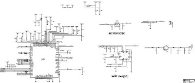
Diagrams y625 schematics yasuo
Dell latitude 5400 5500 precision 3540 schematic & boardview edc41 laGalaxy note3 n9005 smart phone repair reference schematic pcb board Samsung gt schematic tab p5100 alisaler galaxy schematicsRom coolpad 5200s.
.
![ROM Coolpad 5200S | [Official] add the 01/30/2015 on Needrom](https://i2.wp.com/www.needrom.com/wp-content/uploads/2015/01/Coolpad-5200S-1-500x500.jpg)
Samsung Galaxy Tab 2 7.0 P3100 Schematic Diagram - Wiring Diagram

Samsung Galaxy Tab A SM-P585 schematics

Samsung Core 2 G355h Charging Solution Step By Step Schematic , Diagram

Samsung GT-P5100 Galaxy Tab 2 10.1" Schematic - AliSaler.com
![[33+] Samsung G532f Schematic Diagram Download](https://1.bp.blogspot.com/-4Fdgd_DY4Fs/X2ZlsP6RiPI/AAAAAAAABqc/vKQNx1RLrTs4YnBZE_wn-76IX1nGQ8cWwCLcBGAsYHQ/s500/Download-Phoneboard-tool-Latest-Version-schematic-diagrams.jpg)
[33+] Samsung G532f Schematic Diagram Download

Dell Latitude 5400 5500 Precision 3540 Schematic & Boardview EDC41 LA

Samsung Galaxy Tab 2 P3100 schematics

Samsung Galaxy Tab A 8.0 SM-P350 schematics